Saturday, 21 December 2013

Final Big Day of Bachelor of Engineering Technology Students

Before i brief further i want to Thanks to God, family, my supervisor n friends for the prayers, support n guide.Finally done with my own heart beat rate measurement device interface with smartphone via wireless technology. Below is my picture waiting for the lecturer to access me.


The comment from the lecturer is i have to include more analysis or results of my project, such as the analysis or prove that the distance of the bluetooth, difference between the real PPG devices with the TCRT1000 which is optical sensor and Bluetooth signals analysis. I will keep continue with the results and analysis to improve the performance of the results. I have also tabulated table of the results of heartbeat rate of other students, which is as below:

Students
Frequency Average (Hz)
Heart Beat Rate (BPM)
A
1.205
72.3
B
1.316
78.96
C
1.923
115.38
D
769.2m
46.152

The heart beat rate of the students is as below:


Results from Student A (1.205Hz)

Results from Student B (1.316Hz)

Results from Student C (1.923Hz)

Results from Student D (769.2mHz)

The lecturer also comment that, i should also include the students health condition with the results obtained from the students. This i take as improvement of the devices. Further more, the recommendations to improve the device is to change the wireless technology that used. I suggest that, replacing the bluetooth to GSM module so that, it can transmit the data anywhere. 

That's all for now. I will keep updating and research to improve the heart beat device that using wireless technology to transmit the data as to help the community to get the healthier life and easier life. Bye bye for now, and i have to get ready for my final exam. See all you again..Bye

Saturday, 14 December 2013

Getting Ready for Industrial Day

Hai everybody,

I am very excited about the presentation day and i have to refresh back and study about my project which is heart beat monitoring with smartphone via bluetooth. I have to study about how the system works. From the TCRT1000 sensor, process by 2 signal conditioning and transmit it to the smartphone via bluetooth. This week, i will also prepare the casing of the project and final testing of the circuit which is shown in Figure below.


As shown on Figure, the heart beat rate device monitor with LCD and smartphone via bluetooth is done and successful. I am ready for the presentation day. See you all there...

Friday, 6 December 2013

Ready for Final Year Project Presention

The requirement for UniKL BMI on presentation day is a poster about the project. The poster should include as below:


  • Objectives
  • Abstract
  • Methodology
  • Diagram
  • Analysis
  • Results
  • Conclusion
I have make my own poster, which i used power point to do it, and adjusting the paper layout. The step are shown on Figure below.


The full poster of my project that already converted to the pdf format is as below.


Done with the poster, and i'm ready with the presentation. Bye for now...

Saturday, 30 November 2013

Ready for Final Year Project Report

This is almost comes to the end of the Final Year Project, where the project is almost done and we have to do the report about the project. The report should have:


  • Abstract - Summary of research objective, research scope of study and methodology and expected findings
  • Introduction - Overview of project and objectives. Problems identification and the significant of the study.
  • Literature review - The theoretical study and/or recent study from journal and/or relevant resources.
  • Material and Methodology - Materials and methods must support scope of studies. Analysis/ hardware design/case study must be relevant to the objectives.
  • Results/Discussion - Data/graph/calculation/results presentation support the objectives of the study. Data, calculations and derived results are clearly presented. Data accuracy and precision be addressed. Discussion must relate to theory/literature, comparison be made between experimental results and theoretical/predicted/reported values
  • Recommendation and Conclusion - Overall conclusion must be clearly stated along with recommendations for future work.
  • Project Report format/organization - Project report written and organize according to the required format. Content is well organized and coherent.
After the report has been done, hard cover for the report must be include. It is requirement of the UniKL BMI as the report has been completed. The report then submitted to the library of UniKL BMI, which also can be view here http://ir.unikl.edu.my/jspui/handle/123456789/530

That's all by now, next week will be the presentation of the all Final Year Project. See you guys there..

Saturday, 23 November 2013

Testing and Troubleshooting the Wireless Bluetooth PPG

This is difficult task of the week, because it is require more patience and applying all the electrical and electronic plus with communication knowledge to get its done. Before i'm going to explain the real circuit of my PPG, i would like you all to know that, the first circuit of the PPG is not functioning. Previous testing was done and there's a lot of noise and resonant occur as shown on Figure. The figure was taken from the google, just for the example of the noise resonant.


Resonance of a circuit involving capacitors and inductors occurs because the collapsing magnetic field of the inductor generates an electric current in its windings that charges the capacitor, and then the discharging capacitor provides an electric current that builds the magnetic field in the inductor. This process is repeated continually. An analogy is a mechanical pendulum.
At resonance, the series impedance of the two elements is at a minimum and the parallel impedance is at maximum. Resonance is used for tuning and filtering, because it occurs at a particular frequency for given values of inductance and capacitance. It can be detrimental to the operation of communications circuits by causing unwanted sustained and transient oscillations that may cause noise, signal distortion, and damage to circuit elements. This is might because of my circuit not functioning. Plus, the previous PPG was damage because of the over-current injected to the PPG. 
So, for my last minute plan, i have to use other PPG or heartbeat device detector. I get the second PPG circuit from http://embedded-lab.com/blog/?p=5508. I construct the circuit from the web from the beginning by constructing the PCB layout and lastly, testing the circuit. Except that, i add so that i can monitor the heart beat rate. The result is as below.
The circuits consist of 3; 5V voltage regulator with LCD, PPG circuit and Arduino circuit. After the circuit successful get the results that almost accurate, i'm doing the analysis by view the signal by using the oscilloscope. The results that i obtained is as below:

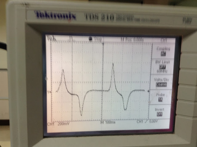
For this circuit, it is without Bluetooth Bee to transmit the data to the smartphone wirelessly. Figure above shows the circuit is operating and display on oscilloscope. The A0 pin of Arduino are connected to the oscilloscope to get the output of the heart beat rate. The output voltage waveform is produce by the heart beat rate circuit. The differences between two beats from the peak value will then measured in term of frequency. From the Figure above, the results obtained is 1.266Hz, then multiply it by 60 to get the Beat Per Minute (BPM) value, which is equal to 75.96 BPM.

I'm also taking the results for the First and Second Stage of signal conditioning. Just want to know how the waveform looks like. Below are the results:
First Stage Signal Conditioning
Second Stage Signal Conditioning

As shown on above, there are difference waveforms which is the waveform at first stage is not detail as second stage of signal conditioning. Then the buffer amplifier is used to transfer a voltage from a first circuit, having a high output impedance level, to a second circuit with a low input impedance level. The interposed buffer amplifier prevents the second circuit from loading the first circuit unacceptably and interfering with its desired operation. In the ideal voltage buffer in the diagram, the input resistance is infinite, the output resistance zero (impedance of an ideal voltage source is zero). Other properties of the ideal buffer are: perfect linearity, regardless of signal amplitudes; and instant output response, regardless of the speed of the input signal.

After the results for the analysis have been done, i'm proceed with interfacing the PPG circuit to the smartphone via bluetooth. I'm using the previous program that i've already post on previous blog. The result is as below:
As you can see, the results of the heart beat rate is appear on the LCD and smartphone. The data will keep transmitting to the smartphone via Bluetooth as long as Bluetooth is ON. The Bluetooth bee must be set to Trans mode so that the data can be transmit. The application Bluetooth SPP.apk which available on PlayStore android should be download as the platform of the device.

I know the circuit is quite messy, and now i have to think the casing of my PPG. See you guys next week.. :)

Wednesday, 13 November 2013

Bluetooth Programming and Testing

Hai Everybody,

This week I'm gonna research how to write programs so that my device can interface with smartphone bluetooth to send data. First of all, i'm gonna used Cytron Bluetooth Bee as shown on Figure.


As shown on Figure, there are Arduino Uno R3 that attached with Xbee Shielding, and top of it is Bluetooth Bee. There are also shows how to connect with the 16x2  LCD and connecting to the PPG circuit. The  Bluetooth  bee  is  supplied  by  3.3V  from  the  Arduino,  while  the  Arduino  is supplied by 5V from the USB port of the computer or from the 5V voltage regulator. To program the ATmega328 of the Arduino, Arduino IDE must be download, because it is the compiler of the system. Figure below shows the one of the screenshot of  the Arduino IDE compiler.


The  figure  above shows  the  Arduino  IDE  software  already  been  installed  on  the computer and it is connected to the COM3 of the computer USB port ready to be programmed.  Arduino  IDE  will  compile  the  sketch  and  upload  into  Arduino  UNO connected to your computer (if there is no error), further run the sketch on Arduino UNO. You will just have to wait until the message box say Upload Done and look at
the Arduino Uno. The red LED are always  blink at 1 second rate  when 5V is supplied to the Arduino. Figure below shows the Bluetooth Bee pin out.

To make sure the Bluetooth Bee is functioning well before proceed with the real program, i search on the Google the simple program. Just to make sure it can at least transmit any data to the smartphone. But first, i'm gonna use Bluetooth SPP.apk one of the applications that can be found on the Play Store of the Android phone. It is platform that can transmit or receive data from Bluetooth Bee. Below are the program that allow transmitting to the smartphone via bluetooth:

#include <AltSoftSerial.h>
#define rxPin 0
#define txPin 1

AltSoftSerial mySerial(rxPin, txPin);

void setup()
{
// define pin modes for tx, rx pins:
pinMode(rxPin, INPUT);
pinMode(txPin, OUTPUT);
mySerial.begin(9600);
Serial.begin(9600);
}
void loop(){
mySerial.print("BPM");
mySerial.print(BPM);
Serial.print("BPM=");
Serial.println(BPM);
delay(1000);
}
delay(80);
}

This program is successful, but i will show on the week that i will presentation day. See all of you there..

Friday, 8 November 2013

Arduino Uno R3 Programming and Testing

Hai everyone,

Until this week, i already did testing one by one of my circuit. Start from the 5V supply, to the LCD, to the Arduino Uno R3 and PPG circuit. As you can see figure below, there are the result.


It is not clear, the LCD printing some words which is "Heart Beat Rate BPM  = (love symbol). As you guys can see, my circuit is working, but now, i have some problem which is the output from the PPG is not appear at the LCD. Theres might be my programming or the circuit design. Still working on it. Wish me luck

Monday, 4 November 2013

Arduino Uno R3 Purchasing

For the time being, i'm just need Arduino Uno R3 for testing the circuit. It is cost RM60 + RM6 for the USB cable. I bought it from Online Component, Jalan Pasar.

 Port that i used are 5V, GND, A0, 12, 11, 5, 4, 3 and 2. More information about the product, you can view at here http://www.myduino.com/index.php?route=product/product&product_id=271.


Friday, 25 October 2013

PCB Etching and Soldering Semi Mounted Device Component

Hi everyone,

This week will be etching process for PPG circuit. Actually this is forth etching, since the etching is not too good before. I've been learn how to etch a PCB by just watching video from youtube, you can view it here http://www.youtube.com/watch?v=RfelrrZyCYQ, it is quite easy if you just watch the video, actually it is really  trivial works. The works is as below:

  1. Put on the goggles and gloves. Always remember safety first because it is deal with acid chemicals.
  2. Make sure the area is well ventilated before mixing. The chemicals will produce hazardous fumes.
  3. Exposed your PCB with the transparent plastic PCB layout at the UV light box for 60 minutes.
  4. Mix two parts hydrogen peroxide for every one part hydrochloric acid. When mixed, they form a substance that is a severe skin irritant, and will produce toxic chlorine gas.
  5. In a non-metallic basin pour enough of the solution to completely submerge the circuit board.
  6. Drop in the circuit board and agitate it for about ten to fifteen minutes. Continue stirring until all copper has dissolve, and the solution has taken on a slight green tinge.
  7. For cleanup, make sure you are wearing gloves. Wash the board off in cold water to remove any etching solution. Then use a paper towel or rag to dry it off completely. Set it aside. Assure that there is no solution in the workspace or containers then remove the gloves and googles.
  8. Mix a one to one ratio of acetone and rubbing alcohol. Take a paper towel, dip it into the solution, and gentle rub it over the surface of the board. The permanent marker will begin to come off. Continue rubbing until all marker is gone. You should see that the circuit is now inscribed in the copper.
Below are my PCB after the etching process.

Next is the assembly process, it is include drilling and soldering as below:
  1. Before drilling locate all the positions of the through hole components.
  2. Drill through the board with a bit wide enough to accommodate whatever part must be placed at that location.
  3. Place the components on the circuit board at their designated locations.
  4. Soldering is a skill that requires practice, although it is not inherently difficult.
You can view this video http://www.youtube.com/watch?v=b9FC9fAlfQE for tutorial of soldering SMD components. Soldering SMD component is hard, that's why i need some items to make the job easier. The item is listed below:

  1. Tweezers
  2. Magnifier
  3. Flux liquid
  4. Solder wick
  5. Solder wire 0.8mm
  6. Solder iron with 0.5 mm tip
Below are my circuit that is still on soldering process.


Finish with the etching and soldering this week, let's go for the testing of the circuit. See you next week.

Monday, 14 October 2013

Bluetooth Research

I'm deciding to use Bluetooth as the wireless data transmitting and receiving to the Smartphone. First of all, i already decided the hardware that i should used. Below are the bluetooth hardware that used for my PPG interface with the smartphone:


  1. Arduino Uno R3, which you can find here, http://www.myduino.com/index.php           route=product/product&path=37&product_id=271
  2. Xbee Shield for Arduino, which you can find here as well, http://www.myduino.com/index.php?route=product/product&path=40&product_id=108
  3. Bluetooth Bee, this is the link, http://www.myduino.com/index.php?route=product/product&path=50_56&product_id=105
Thanks for keep updating my blog.


Thursday, 10 October 2013

PCB Design

Hai there,

After few weeks keep researching on how to etch a PCB, this week is my first time designing a PCB using Proteus software. Designing a PCB quite difficult, because i have to draw back all the circuit at the Proteus software then convert it to ARES. When it comes to ARES format, i have to arrange all the component and avoid wire jumper as possible. Below are my Proteus (ISIS) and ARES that already converted to the PCB layout.


Notice the circle mark, it is supposed to be LT1932, but its not available at Proteus. So, to solve this problem is, i just have to make footprint at the ARES which you can see at figure below.

Before etching the PCB, make sure all the component is fit at each soldering point or solder resist. On the left side is the upper and the right is bottom of the PCB. That's all for this week, see you guys next week.

Tuesday, 1 October 2013

Current Stabilier and Operational Amplifier OPA2350

Good Evening everyone,

Finally, my LT1932 current stabilizer and Op-amp OPA2350 have arrived. For your information, this is very rare components, its hard to find unless ordered or purchase online.

LT1932
In the previous post, i have post the datasheet of LT1932. At this post, i will summarize the LT1932. The function of LT1932 is used for stabilized the IR LED current to obtain the visible light output gain accuracy. LT1932 Constant Current DC/DC LED Driver in Thin SOT is used for the purposed of stabilizing the current that drives the LED and the appropriate resistor values a shown in Table below

LED Current (mA)
Resistor Value
40
562Ohm
30
750Ohm
20
1.13kOhm
15
1.5kOhm
10
2.26kOhm
5
4.53kOhm

So, the desired value that we expected is 20mA and i should used 1.13kOhm resistor at pin Rset or pin no 4 of LT1932.

The results of IR LED resistor current test is shown in table below.

I LED (mA)
R set Value
25.4
1kOhm
18.2
1.3kOhm
15.7
1.5kOhm

Figure below shows the actual component of LT1932.

OPA2350
This component also is the rare component, and i ordered it together with the LT1932. The datasheet of OPA2350 can be found here http://www.ti.com/lit/ds/symlink/opa2350.pdf. Actually, OPA2350 have 2 input and 2 output. In the circuit diagram, it is label by A and B for example OPA2350 U1:A and OPA2350 U1:B. Figure below shows the OPA2350 diagram.


It is show that for output A is using terminal 1,2,3,4 and 8. For the output B is using 4,5,6,7 and 8.

Figure below shows the actual component of OPA2350


The cost of both components is list at table below.
Component
Quantity
Price
LT1932
1
20.00
OPA2350
1
25.00
                                Total
45.00

The price is quite expensive because the items is seldom and hard to find. But for the successful of the project, there are no other option to make its successful, one word for it SACRIFICE. See you next week.. :)


Friday, 27 September 2013

Purchasing Item

Welcome Back!

Everything is on schedule, i already purchasing component for my PPG circuit. Figure below shows the component that i had bought.


As can be seen in the Figure, the Surface Mounted Device (SMD) components is small. It is not more than 5mm width and 3mm length, and it is totally different with through hole components. This method for producing electronic circuits in which the components are mounted or placed directly onto the surface of Printed Circuit Boards (PCBs). There are no leads or either smaller leads and it may have short pins or leads of various style.

Why is choose SMD as component for the PPG circuit is
  • Smaller components.
  • Lower initial cost and time of setting up for production.
  • Fewer holes need to be drilled.
  • Small errors in component placement are corrected automatically as the surface tension of molter solder pulls components into alignment with solder pads.
  • Lower resistance and inductance at the connection; consequently, fewer unwanted RF signal effects and better and more predictable high-frequency performance.
  • Better EMC compatibility (lower radiated emissions) due to the smaller radiation loop area and the smaller lead induction

The cost of all the item purchased is shown on table below:


The cost of all the item purchased is shown on table below,. 
Components
Value
Quantities
Price (RM)
Capacitors (tantalum or ceramic, voltage rating?) below 50V
4.7uF
1uF
 12pF
10uF
10
2
1
1
8.00
3.00
1.50
2.30
Inductor
6.8uH
1
2.80
Resistors
1kohm
1.3kohm
22kohm
1Mohm
10
10
10
10
1.00
1.00
1.00
1.00
Diode Schottky (20V 1 A)
1 A,40V
2
8.00
Diode Zener
5.1V
2 pieces
4.80
LED
5V
10
2.00
  Total                                    
36.40
The total for the components is not much and it is affordable. But, the LT1932 and OPA2350 i have to order because it is seldom used and the stock is not in the electronic shop. The ordered have been made, and i have to wait for 3 working days for the components to arrive. Below are the list of the electronic shop where is purchasing the item:
  1. Online Component Sdn. Bhd. (www.online-components.com.my)
  2. MSC Supply and Service 
Any rare components can be found at MSC Supply and Service, credit to this company because almost half day searching for the LT1932 and OPA2350 and it only be found and can be easily ordered at that electronic shop. That's all for now. Thank You.. See u Next Week..


Thursday, 19 September 2013

Circuit Simulatioin

When its come to simulation, there's many things that i think how i should simulate the circuit. So, after keep asking Mr. Google, finally, its come to solution. The solution is i have to test the circuit 1 by 1. From the First circuit, the IR LED Current Stabilizer, Second circuit is Trans Impedance circuit and the last circuit is sallen key filter circuit. The result should be almost the same as theory result that i found in the article. Figure below shows the circuit and its result. I skipped the IR LED current stabilizer simulation, because i can't found LT1932 component, and plus, my supervisor assure the circuit will have no problem if the connection is right, because the circuit is original from the datasheet of the LT1932 which you guys can view here http://cds.linear.com/docs/en/datasheet/1932f.pdf.

Transimpedance Circuit 
Started with the trans impedance circuit simulation, you can see figure below:

Figure above shows the simulation circuit for trans impedance circuit. It is using Proteus for the simulation software. As can be seen it is 1.5V supply to the circuit and resulting 24.01mV. A transimpdance amplifier is an amplifier that converts current to voltage. Its input ideally has zero impedance, and the input signal is a current. Its output may have low impedance or in high-frequency applications, may be matched to a driven transmission line, the output signal is measured as a voltage. I assuming that the input voltage is 1.5V from the IR LED Current stabilizer and it is supposedly current. The noise gain for example the noninverting closed loop gain of this configuration determines the stability of the circuit. The reason for this is that any noise signal, no matter how small, can trigger an unstable circuit into oscillation. The DC gain is set solely by the resistors. The pole frequency is set by the feedback network, just as in the impedance function. Table below shows the current input and output for the transimpedance circuit.

Current Input (mA)
Voltage Output (V)
0.010
0.01
0.022
0.02
0.031
0.03
0.04
0.04
0.052
0.05
0.061
0.06
0.072
0.07


Sallen Key Low Pass FIlter
The second circuit is sallen key low pass filter. See figure below:

The circuit above is simulated using Multisim software. It is hard to simulate using Proteus, so i come with the solution by using Multisim. As can be seen, i'm not using OPA 2350 for the operational amplifier. Supposedly it is OPA 2350, but, i can't found it inside Multisim. As my supervisor advised, it is almost the same amplifier, as long as the result is there. So the function generator is set to 5V amplitude and the Frequency is set to 5Hz.
The sallen-key filter is a simple active filter based on utilizing op-amp stages, which is ideal for filtering analog frequencies. It is one of the most widely used filter topologies. One reason for its popularity is that this configuration shows the least dependence of filter performance of the performance on the performance of the op-amp. Another advantage of the configuration is that the ratio of the largest resistor value to the smallest resistor value and the ratio of largest capacitor value to the smallest capacitor value are low, which is good for manufacturability. A serious drawback is that the filter is not easily tuned. A low pass filter is a filter that passes low frequency signals but attenuates signal with frequencies higher that the cutoff frequency. Desire cut off frequency is 10 Hz which can be seen on the simulation, i get the 10 Hz cut off frequency.


As a summary, the both amplifier play important role to in very low frequency applications and it is commonly used in receivers for optical communications.

That's all by now.. Thank you.. Keep in touch..


Thursday, 12 September 2013

Hai Everyone, How are you? This is First week for my final year

Continue from Week 14,

Hai everyone, i'm getting ready to start new semester, and this is my final year here at UniKL BMI. Once again, this is Final Year Project and this semester will start to busy to purchasing component, constructing, testing, troubleshooting and presentation for the project. Usually for the first week of the semester, still relax and introduction of the chapter. In this week, i'm gonna meet my Supervisor Sir Saiful Yusri to get refresh about the project. What i should this final semester for my Final Year Project 2 is:


  1. 9 - 13 September 2013, First Week - Meet Supervisor
  2. 16 - 20 September 2013, Second Week - Test the circuit using simulation
  3. 23 - 27 September 2013, Third Week - Purchasing component
  4. 30 September - 4 October 2013, Forth Week - Ordering component LT1932 and OPA 2350
  5. 7 - 11 October 2013, Fifth Week - Design PCB
  6. 14 - 18 October 2013, Sixth Week - Bluetooth Research
  7. 21 October - 25 October 2013, Seventh Week - PCB Hatching and Soldering SMD Component
  8. 28 October - 1 November, 8th Week - Bluetooth Purchasing
  9. 4 - 8 November 2013, 9th Week - Android Programming and testing
  10. 11 - 15 November 2013, 10th Week - Bluetooth Programming and testing
  11. 18 - 22 November 2013, 11th Week - Testing and troubleshooting the wireless Bluetooth PPG
  12. 25 - 29 November 2013, 12th Week - Ready for Final Year Project Report
  13. 2 - 6 December 2013, 13th Week - Ready for Final Year Project Presentation
Hope all is running on track. Wish me the best in this semester!! See you next week.

Tuesday, 23 April 2013

Received PPG from My Supervisor

Dear All,

Actually today i'm not feeling well, it have been 2 days of dizziness and i don't have mood to have my lunch and dinner. Well, that's life. I met my supervisor this afternoon at 2.30 pm because he asked me to take the PPG devices. Before handover to me the PPG, we discuss a bit about the PPG and circuit need to be constructed.


Inside the PPG there are LED DC Current Source and Photodetector, while the end of its is 9 pin "D" connector of male. The brand of the PPG is NELCO oximeter finger probe. Sir Saiful Yusri which is my supervisor explained to me about the functions of the connecter pin which is as table below:-


Connector End Pin
Pin Name
Description
9
Phototransistor cathode
Green wire
5
Phototransistor anode
White wire, phototransistor detects level of IR and/or red light transmitter through the finger
2
LED1
Red wire, anode of the IR LED, cathode of the red LED
3
LED2
Black wire, cathode of the IR Led, anode of the red LED


Those are important configuration pins because all of its link to the filter circuit, amplifier and interface with microcontroller.


To make this works, we need IR LED current stabilizer LED current is between 5mA and 40mA. We will used LT1932 circuit for it. Therefore, for the transimpedance, we choose this because photodiode will produces a strong tendency for the amplifier to go into oscillation at some high frequency above the gain bandwidth cutoff. This problem can be eliminated by adding a small capacitor in the feedback loop, which lowers the gain at very high frequencies. For the filter circuit we'll we use the Sallen-Key Low Pass Filter which are buffer circuit. And the output of it will interface with the microcontroller which will send the signal to the Smartphone using GSM.

That's all for now......See you again...Will come back in next week probably..

Friday, 19 April 2013

Project Proposal Preparation

Week 13,

Day pass by really pass, now is week 13, and we have to prepare for project proposal which need to be submit by next week. Actually, the my proposal have been prepared for the last 3 weeks before, and at this week i just need to check it all and see which part i should add more. Below are my contents of the proposal.


Contents
1.0 introduction.. 2
1.1 About Heart Rate. 2
1.2 What is Photoplethysmography?. 2
1.3 Background of the Project. 3
2.0 problem statement.. 4
2.1 Design that Inhibits the Ability. 4
2.2 Expensive. 4
2.3 Limit Range. 4
3.0 aim and objectives. 5
4.0 project scope and limitation.. 6
4.1 Project Scope. 6
4.2 Limitation.. 6
5.0 expected outcome. 7
6.0 literature review... 8
6.1 References from Article. 8
6.1.1 Title: Portable Heart Rate Detector Based on PPG with Android Programmable Devices for Ubiquitous Health Monitoring System... 8
6.1.2    Title: Wearable Wireless Photoplethysmography Sensors. 8
6.1.3     Title: A Wireless Cardiovascular Monitoring Device and Its Clinical Tests. 9
6.1.4  A Real-Time Cardiac Arrhythmia Classification System with Wearable   Sensor Networks  9
7.0 methodology.. 10
7.1 Android Application.. 10
7.2 Wearable Sensor. 11